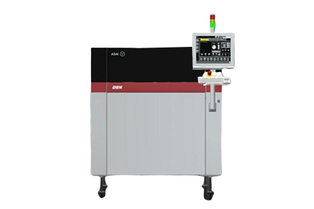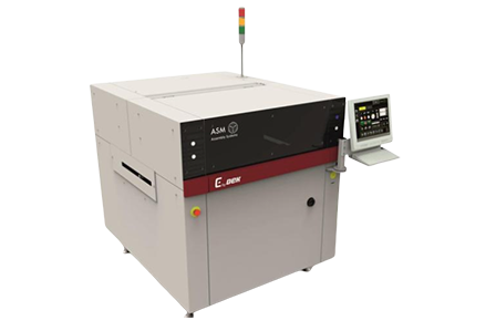


Close to customers

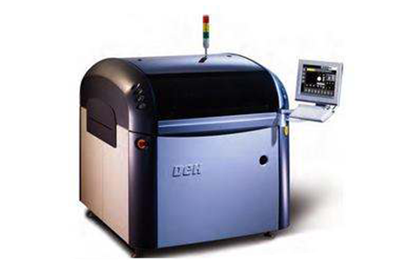
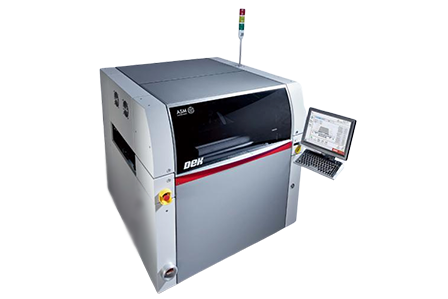
As a latecomer, if you want to make a difference in the field of semiconductors gathered by experts, you must have a different strategy. Shen Huipan said that the DEK approach is "close to customers as much as possible to understand their new needs." In fact, these are also reflected in the company's product line configuration-in addition to large equipment, this time they also have an extensive process support product (PSP) line. Shen Huipan introduced the four stencils of DEK the matching VectorGuard frame system.
Platinum stencil, Gold stencil, Silver stencil 3D stencil are the four stencils that DEK mainly promoted at this exhibition. Although the purpose of this trip is mainly to promote to semiconductor manufacturers, like Photon Galaxy, these four screens can also be used for SMT equipment.
If you want to talk about cost accuracy, the first thing is naturally Platinum. Shen Huipan introduced that this type of stencil is very suitable for ball implantation of wafers over 8 inches, the pitch is less than 0.3mm. "Of course, it can also be used for 0.5mm 0.6mm pitch ball planting, but many devices can already meet this point. Only under 0.3mm can you take advantage of the Platinum screen." He said, "regardless of the angle of the opening, Size accuracy, we can all make it very small, so as to meet the ball planting process below 0.3mm-we have seen 0.07mm ball planting process in the market, in fact, only the Platinum screen can meet this process Requirements. Of course, its price is also higher. "It is reported that as the diameter of the ball the distance between the balls continue to shrink, the screen mesh between the screen holes is becoming smaller smaller, which requires the screen material. . This is the advantages of Platinum stencils lie.
Gold stencil Silver stencil are both nickel stencils. The difference lies in the processing method-the former is an electroformed stencil obtained by electrochemistry, the latter is obtained by mechanically cutting the nickel plate. Shen Huipan pointed out that the finish of the hole wall of the latter is slightly inferior, but its advantage is that the processing time is much shorter than the former. "Customers can choose between time performance based on their actual needs," he said. However, he also acknowledged that if the acceleration can be reduced as much as possible during the demolding, manufacturers can obtain better product performance even with Silver stencils. However, the price paid for this is "the time advantage of the Silver network board has disappeared." It is reported that the cost difference between Gold stencil Silver stencil is 6 times. "But if the added value of the product is large large-scale mass production is possible, this gap can be completely digested." Shen Huipan said.
If a chip already exists on the substrate being printed, how can the manufacturer perform screen printing without damaging the existing chip? The answer is the customizable 3D network board service launched by DEK. It is said that this is also a stencil obtained using the electrochemical principle. For customers who choose this technology, DEK can also customize special metal scrapers for them.
In addition to the stencil, DEK did forget to promote its VictorGuard frame technology. It is said that the detachable screen using this screen frame can save the stretching of the screen due to the corrosion of the screen during cleaning due to the elimination of the screen stretching process. It can also save a lot of space reduce the storage of the screen. Inventory costs. Shen Huipan pointed out that although the cost of this frame is relatively high, considering the future storage, manufacturers can fully absorb this cost. It is claimed that this technology already accounts for 12% of the global market. "As a DEK patent, we are also trying to contact other stencil vendors in the market sell patent licenses to expand the market for this technology." Shen Huipan said, "I hope it will become a development trend of stencil technology. "
13962439646
Address: No. 259 Songjiagang Road, Zhoushi Town, Kunshan City, Suzhou City, Jiangsu Province
Email: srd@kunshansmt.cn