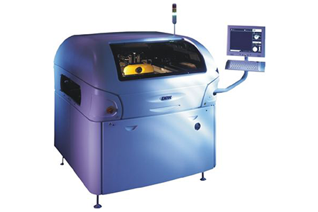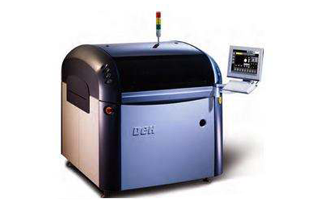


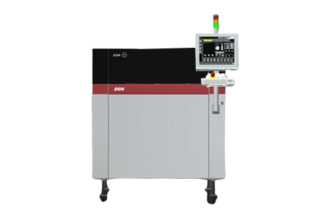
Cutting-edge DEK printing press development
DEK redefines acceptable capacity, utilization cost parameters in advanced semiconductor packaging.
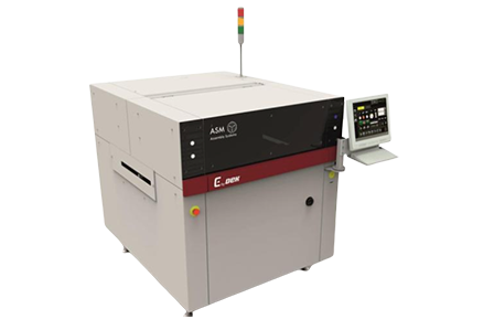
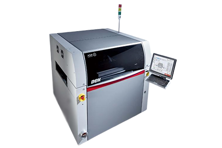
We have proven that when it comes to wafers, batch printing can handle high-precision processes- it has won industry awards. Thanks to the expertise of closed print heads, we have developed solutions for a wide range of packaging processes. we have created new processing methods for semiconductor processes, which can be easily integrated into customers' existing assembly processes.
Our value

As a developer of advanced technologies services, we use our skills experience to turn inspiration into reliable repeatable products that truly add value to our customers' activities.
We have won the trust of our customers as a reliable business partner, consistent consistent performance in the world's electronics industry, a consistent commitment to providing the best possible business practices.
"As a customer's partner, our goal is always to be as open responsive as possible. We strive to continuously develop optimize network resources so that you can obtain DEK product process support, order online, directly enter DEK worldwide organizations A window to the structure. Anything about the DEK website DEK business, you can directly email me. "DEK, a British electronics manufacturing equipment supplier, demonstrated its tradition to the electronics manufacturing industry at Semicon China in Shanghai a few days ago. A completely different image. Relying on the original Galaxy Photon platforms, the company brings solutions for semiconductor wafer-level printers. Shen Huipan, general manager of DEK China, stated clearly that its business focus will be on the semiconductor field. In addition, BTU, an alternative energy process equipment supplier, also opened the photovoltaic technology innovation center in Shanghai Waigaoqiao during this period. The production line equipment shown was based on the PVP1200 screen printing machine provided by DEK. There is no doubt that DEK is ready to diversify its business is making great strides in the semiconductor solar energy fields.
13962439646
Address: No. 259 Songjiagang Road, Zhoushi Town, Kunshan City, Suzhou City, Jiangsu Province
Email: srd@kunshansmt.cn