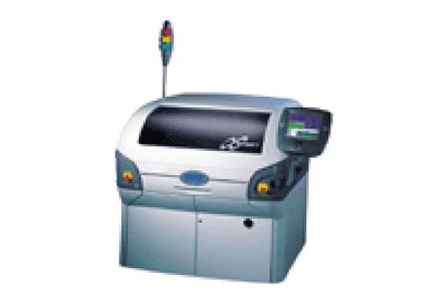

DEK printing press solution
Approaching DEK's booth at Semicon, the most eye-catching are three devices: a Galaxy press, a Photon press, wafer processing equipment (provided by CHAD) that can be used with them.
The first to introduce is the wafer back printing solution based on Photon printer. According to the information provided by DEK, this solution uses DEK's high-speed synchronous pattern recognition technology mature high-quality position encoder technology. The former helps reduce fiducial point alignment board positioning time, while the latter enables repeatable printing for wafer-level chip-scale packages 01005 components. Shen Huipan, general manager of DEK China, said that the advantage of the Photon platform is its high flexibility, which is also reflected in this feature. Shen Huipan said that this solution can support the printing of various liquid materials including epoxy resin glue. "There are up to 3 to 5 known printing materials. But as technology develops, the needs of manufacturers are changing." He said, "When manufacturers propose to print a new material with different viscosity other characteristics, At that time, equipment manufacturers have to adapt to the situation. Obviously, Photon has already done this. "
DEK announced the micron-level high-end screen printing machine Galaxy at Semicon China in 2004. This time, the semiconductor ball planting solution with DirEKt printing technology was displayed. Shen Huipan said that customers have been able to mass-produce balls with a diameter of less than 0.25mm (such as 0.17mm) based on this equipment. He went further said that the company he worked for has already realized the production of 0.07mm diameter laboratory bulbs based on Galaxy presses. "But given the specific nature of the semiconductor industry, we need to conduct further research on yield issues," he said.
The wafer processor provided by CHAD is placed between the two printing presses mentioned above-no matter whether it is a backing a ball, this processor can calculate the number of wafers complete the final positioning according to the manufacturing requirements.
"The wafer processor actually plays the role of a robot." Shen Huipan said. He said that the reason why the equipment was exhibited together was to show the value that DEK brings to electronics manufacturers in terms of high flexibility. "As technology advances, the electronics manufacturing requirements for equipment are constantly changing. They may have such requirements today, tomorrow they will have the same requirements. Obviously, a machine with a single function cannot It meets such changing requirements of users. "Shen Huipan explained," The value of DEK is here-the same printing press, after different configurations, can achieve different functions, such as coating ball placement. "
13962439646
Address: No. 259 Songjiagang Road, Zhoushi Town, Kunshan City, Suzhou City, Jiangsu Province
Email: srd@kunshansmt.cn
